Microscopy Techniques
The CM group uses a range of microscopy techniques including STM, AFM, MFM, SEM and TEM.
Multi-technique Cryogenic Surface Probe Microscope
Our latest acquisition arriving March 2019 is a multi-technique cryogenic surface probe microscope funded by the UK Engineering and Physical Sciences Research Council strategic equipment grant. This unique instrument combines atomic force, magnetic force and scanning hall probe microscope stages into a He-3 cryostate with a base temperature of < 400 mK and a vector magnet that can supply 1T mangetic field in any direction, or 5T in a vertical orientation. The microscope is also equipped with dc and rf transport lines to the cold stage allowing us to perform simultaneous imaging and electrical transport measurements. The capabilities are further enhanced with a scanning optical stage option to allow optical excitation of samples as well.
We plan to develop this instrument further with the addition of a scanning SQUID (Superconducting Quantum Interference Device) head to the system.
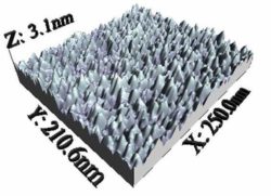
CoFeB thin-film surface imaged using STM.
Scanning Tunnelling Microscopy (STM)
STM is a direct method of characterising clean conducting surfaces that works on the quantum mechanical principle of vacuum tunnelling. It provides information about the topography and local density of states of a surface.
The CM group has a range of STMs including an in-situ measurement for the structural characterisation of layers grown in the MBE system.
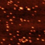
Co nanoclusters imaged with AFM.
Room temperature Atomic Force Microscopy (AFM)
AFM is used to determine surface topology. A sharp tip attached to a cantilever is scanned across the surface of the sample. The deflection of the cantilever, which occurs due to attractive molecular forces, depends critically on the separation of tip and sample and can be used to determine the topography.
The group has access to a range of AFMs with a variety of scan ranges and resolutions.

Magnetic domains imaged using MFM.
Variable Field Magnetic Force Microscopy (MFM)
MFM is similar in principal to AFM, but uses a magnetised tip. The cantilever deflection now also depends upon the magnetic force between tip and sample. An MFM measurement contains information about the magnetic structure of the sample surface.
The CM group uses MFM to image domain patterns and domain walls and nanofabricated devices. One of the MFMs we have access to additional has a variable applied field to allow imaging under applied field conditions as well as preparing defined magnetic states.
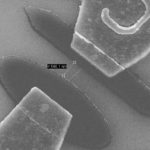
SEM image of a carbon nanotube device.
Scanning Electron Microscope (SEM)
SEM systems scan a focussed beam of electrons across the surface of the sample. The beam, which is focussed to a radius of the order of nm and steered using variable magnetic fields, generates secondary electrons when interacting with the atoms in the sample. The number of secondary electrons yields information about the sample surface and is used to construct an image.
The CM group has one high resolution SEM, situated in the Nanoprobe system described below, and has access to others situated in the Engineering Faculty and University cleanrooms.
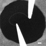
Manipulation of a carbon nanotube.
The Nanoprobe
The Nanoprobe system contains four STM tips and a high resolution SEM. This allows simultaneous SEM operation and tip movement, and is used to assemble nanoscale devices that integrate carbon-based materials with lithographically patterned metallic structures.
The Nanoprobe system is unique in the UK.