Topological Materials
What is topology in the condensed matter physics?
The Nobel Prize in physics 2016 has been awarded “for theoretical discoveries of topological phase transition and topological phases of matter”. Topology is a geometric property that cannot be changed by any continuous deformations. It is necessary to be cut or torn apart in order to go from a cylinder ring state with two distinguishable surfaces to a Möbius strip one with an undistinguishable surface via a non-ring state (see Fig. 1). In other words, the properties described by different topology are topologically protected and can be changed only through the topological phase transition (TPT).
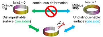
Fig. 1 Topology & geometry. Cylinder ring and Möbius strip states are topologically different.
One can consider a similar topology in the electronic band structures (EBS) of a crystal sample in the reciprocal space. The EBS of the occupied states (below the Fermi energy EF) can be visualized with the angular resolved photo emission spectroscopy (ARPES) using the photoelectric effect as shown in Fig. 2.
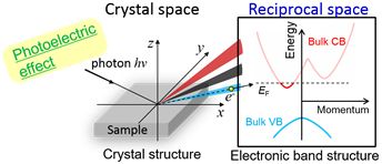
Fig. 2 Real (crystal) space & reciprocal space. The photoelectric effect can be used to visualize the electronic band structures of the conduction bands (CB) and the valence bands (VB) of a crystal in the reciprocal space.
Figure 3 indicates a typical EBS of ordinary (or non-inverted) band insulators (OBI; top left) and exotic band-inverted insulators (BII; top right) with a band gap. Their electronic properties are topologically distinguished and protected by the presence of the band gap. Strong spin-orbit interaction, if tunable, would be able to close the gap of an insulator (therefore non-insulating, i.e., metallic state) and reopen another gap (therefore another type of insulators) through the TPT similar to the case in the real space in Fig. 1. Fig. 2 Real (crystal) space & reciprocal space. The photoelectric effect can be used to visualize the electronic band structures of the conduction bands (CB) and the valence bands (VB) of a crystal in the reciprocal space.
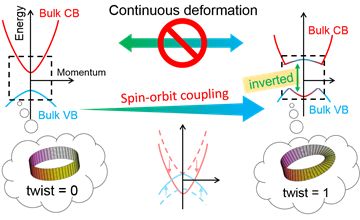
Fig. 3 Topology in the electronic band structure. Ordinary band insulators (OBI; top left) cannot be continuously deformed to any band-inverted insulators (BII; top right).
When two insulators with different topology meet, the TPT has to happen at a heterostructure interface between an OBI and a BII in order to spatially alter the topology in the EBS. The existence of the boundaries is topologically protected. The interface must be non-insulating thereby gapless metallic states as indicated in Fig. 4. In a case that OBI is either vacuum or an ambient atmosphere, the interface, i.e., the surface of BIIs are metallic and the surface states (SS) are topologically protected. Hence, the BIIs are called topological insulators (TI) and the surface of the TIs can conduct though they are band insulators in the bulk (see Fig 5). Moreover, strong spin-orbit coupling makes spin and momentum perpendicularly locked each other in the gapless states as illustrated in Fig. 6.

Fig. 4 Insulators heterostructure & band inversion.
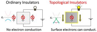
Fig. 5 Topology & electronic conductance
This spin-momentum locking can induce novel phenomena in TIs. For example, pure spin currents with no charge current flow at the surfaces, topological magnetoelectric effect, the image magnetic monopole effect, and the existence of axion (exotic quasiparticle) are expected to be demonstrated in TIs (see Fig. 6). Fig. 4 Insulators heterostructure & band inversion. Fig. 5 Topology & electronic conductance
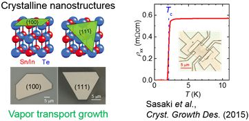
Fig. 6 Novel phenomena expected in topological insulators.
What are real materials for the TIs? Bismuth selenide (Bi2Se3) is one of the typical TIs and we can grow a high quality large bulk single crystal here in Leeds. Figure 7 shows a cleaved surface of a high quality bulk single crystal of Bi2Se3 grown in a vertical tube furnace using a modified Bridgeman method.
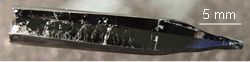
Fig. 7 High quality bulk single crystal of topological insulator Bi2Se3.
Another interesting topic on TIs is adding the superconductivity on TIs as illustrated in the equation in Fig. 8. TIs or the metallic surface states of TIs can superconduct by either increasing the carrier density by chemical doping or using the superconducting proximity effect. The most interesting question is that what kind of superconductivity would realize there. These routes for the topological research may allow us to explore Majorana physics that would contribute to topological quantum computation a future quantum technology. Our current target material is a topological crystalline insulator (a cousin of TIs) tin telluride (SnTe) that can superconduct by indium (In) doping. Figure 9 shows crystalline In-doped SnTe nanostructures grown by the vapour transport method and the superconducting transition of its single crystal nanostructure.
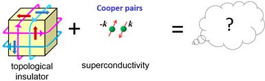
Fig. 8 Majorana physics; topology + superconductivity =?

Fig. 9 Superconductivity of a superconducting topological crystalline insulator In-doped SnTe nanostructure.