Fabrication
Many of our experiments investigate the lateral movement of spin information via the motion of a magnetic domain wall, a spin-polarised current or a pure spin current. In order to access these phenomena, which sometimes only persist over a few nm, we use lithographical techniques to pattern thin films into nanoscale structures.
The figure below shows a six stage lithography process known as electron beam lithography.

The substrate is initially covered in an electron-sensitive polymer known as resist. A pattern is then written into the resist by steering a focussed beam of electrons across the surface of the sample. Those regions exposed to the electron beam are then removed from the resist after development, leaving a layer of resist with a template-like structure. Thin films are then deposited atop this layer of resist. Finally, the resist is removed by a process called lift-off, leaving only the material that was deposited through the template.
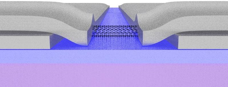
Using the lithography process described above we are able to integrate novel nanoscale materials into our device structures. For example, the figure below shows how a lithographically patterned device can be used to investigate the electrical properties of a carbon nanotube. This device requires two separate lithography stages - one each for the bottom and top contacts which have to be carefully aligned to one another - and the precise placement of a carbon nanotube.
In the Condensed Matter Group at Leeds we use three principal lithography techniques; electron-beam lithography, photolithography and ion-beam lithography. These facilities are part of a state-of-the-art fabrication suite situated in the University's Wolfston cleanrooms.