Giant Magnetoresistance
The Giant Magnetoresistance (GMR) was discovered independently in 1988 by the groups of Albert Fert and Peter Grunberg. It is the phenomenon where the resistance of certain materials drops dramatically as a magnetic field is applied. It is described as Giant since it is a much larger effect than had ever been previously seen in metals. It has generated interest from both physicists & device engineers, as there is both new physics to be investigated and huge technological applications in magnetic recording and sensors. In 2007, Fert and Grunberg were awarded the Nobel Prize for their work on GMR.
Giant magnetoresistance has been the subject of a huge international research effort due to the numerous technological applications. The largest is in the data storage industry and IBM were first to market with hard disks based on GMR technology although today all disk drives make use of this technology. On-chip GMR sensors are available commercially from Non-Volatile Electronics who were the first company to sell GMR products. Other applications are as diverse as solid-state compasses, automotive sensors, non-volatile magnetic memory and the detection of landmines.
Albert Fert receives an honorary doctorate from the University of Leeds
The effect is most usually seen in magnetic multilayered structures, where two magnetic layers are closely separated by a thin spacer layer a few nm thick. It is analogous to a polarisation experiment, where aligned polarisers allow light to pass through, but crossed polarisers do not. The first magnetic layer allows electrons in only one spin state to pass through easily - if the second magnetic layer is aligned then that spin channel can easily pass through the structure, and the resistance is low. If the second magnetic layer is misaligned then neither spin channel can get through the structure easily and the electrical resistance is high.
To get a little more technical, the band structure in a ferromagnet is exchange split, so that the density of states is not the same for spin up and down electrons at the Fermi level. Fermi's golden rule states that scattering rates are proportional to the density of states at the state being scattered into (in this case the Fermi level), so the scattering rates are different for electrons of different spin. These ideas were used as early as 1936 by Sir Neville Mott to explain the sudden decrease in resistivity of ferromagnetic metals as they are cooled through the Curie point.
The GMR effectively measures the difference in angle between the two magnetisations in the magnetic layers. Small angles (parallel alignment) gives a low resistance, large angles (antiparallel alignment) gives a higher resistance. It is easy to produce the state where the two magnetic layers are parallel - simply apply a field large enough to magnetically saturate both layers. But how do we acheive an antiparallel state? There are three basic ideas used here:
1. Antiferromagnetic coupling:
When the spacer layer is extremely thin the sense of the coupling between the two layers oscillates. In other words, for certain specific values of the spacer thicknesses the magnetisations of neighbouring layers will naturally wish to lie in opposite directions. By applying a large enough magnetic field we can force the magnetisations of the layers to all line up along the field direction. In this way it is possible to get the two differentent resistance states. It's possible to build up multilayered structures called superlattices which work on this principle - they are samples where you have a magnetic layer and a non-magnetic spacer repeated many times, e.g. {Co/Cu} x 30. Each magnetic Co layer is separated from it's neighbours by a thin Cu spacer.
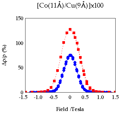
The figure above shows the GMR of a sample with 9Å thick Cu spacers - where antiferromagnetic coupling is strongest. In zero field the resistance is high as all the Co layers line up anti-parallel, and as a field is applied they progressively align, until the sample is saturated. The resistance is then at a minimum at fields larger than this. The red curve is measured at 4.2K, whilst the blue curve is at room temperature (~300K). The room temp GMR is 75% whilst we have 130% GMR at 4.2 K
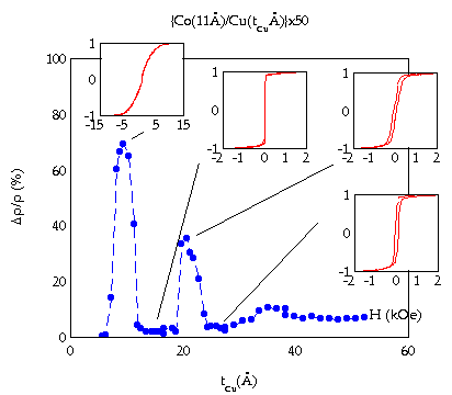
The figure above shows the dependence of the GMR on the thickness of the Cu spacer. There are 3 peaks visible, although only the first two are very strong. At large thicknesses the samples are decoupled, and small random differences between the layers give a small GMR. When the layers are ferromagnetically coupled, the GMR is zero. Notice that the first peak is at a Cu thickness of only 9Å - a copper atom is about 3Å across. Depositing such thin layers without pinholes has only become possible recently with advances in UHV deposition technology. This data was taken at room temperature, and the inset panels show MOKE loops of various samples exhibiting different kinds of coupling. Ocillations in GMR as a function of copper spacer layer thickness.Samples like this have the largest GMR of all - the reason is to do with the mean free path of the electrons which carry the current. (Mean free path is the average distance an electron will travel between scattering events - the longer it is the lower the resistance.) It possible for electrons of appropriate spin to pass through many aligned magnetic layers and have a very long mean free path. This means that the distance between scatters is increased the most when the layers become magnetically parallel. However in most cases they are inappropriate for senor applications, as the fields required to observe the magnetoresistance are very large.
2. Different Coercivities:
If we use two different materials with different switching fields then as we apply the reverse field one layer will switch before the other - we then have the desired anti-parallel alignment. In practice the contrast between the layers has to be good, and most materials do not switch sharply enough to get the full benefit from this technique. We have grown {Co/Cu/Fe/Cu}xN multilayers by MBE which show this sharp switching behaviour. These types of structures are sometimes called 'pseudo' spin valves.
3. Exchange biasing & spin-valves:
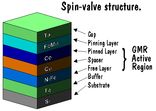
In Leeds we published a number of papers on GMR magnetic field sensors made using spin valve structures. These devices rely on exchange-biasing. It is possible to exchange couple one of a pair of magnetic layers to another back layer of antiferromagnetic material. In the diagram below an FeMn layer is used to 'pin' the Co layer magnetisation in a certain direction. This layer is used as a reference layer. The NiFe layer, which is very magnetically soft, can now be aligned parallel or antiparallel by very tiny fields. There is a thick enough Cu spacer between these two to stop there from being any magnetic coupling between the layers. The Ta layers are a buffer (to give a good surface to grow on) and a cap (to stop the sample from being oxidised in air). The whole sample is deposited on a piece of Si wafer, which is in fact many thousands of times thicker than the whole multilayer structure. The GMR active region will be only about 100Å thick, with the whole structure being about 300Å, on top of a 1mm thick piece of Si. The magnetisation in the Co layer is pinned by the last plane of spins in the antiferromagnet, causing it to be unaffected by small fields applied in this direction. This means that there is effectively a local magnetic field applied to the pinned layer, causing it to be fully saturated at zero field. The magnetisation in the layer actually reverses about some point biased away from zero, due to the effective field. These type of structures are very sensitive to magnetic fields, and are being researched heavily by the magnetic recording industry for use in high density disk and tape playback heads by companies such as IBM and Seagate. Other applications include avionic compasses, swipe-card readers, wheel rotation sensors in ABS brakes, and current sensors for use in safety powerbreakers and electricity meters. To learn more about spin valves click here.