Thin Films Tutorial
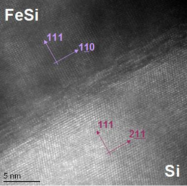
The term thin film typically refers to a layer of material with a thickness less than 1 micron (1/1000 of a mm), but many of the samples studied in our research are as thin as a few nanometres – or tens of atomic layers. The figure below shows the atomic planes in an FeSi thin film deposited upon a Si substrate.
Thin films have a huge range of application and are used in industries as diverse as construction, aerospace and information storage. They are commonly used to modify the surface properties of a material, for example as low-friction, anti-corrosion or highly reflective coatings. The Condensed Matter Physics group specialises in the deposition of magnetic multilayers where several thin film layers are deposited atop one another to form devices such as the spin valve – the basic technology underpinning hard-drive read heads.
The success of these multilayer structures relies upon the growth of high purity, defect free layers separated by clean interfaces and requires some very specialised techniques. In the Condensed Matter Group we mainly use two: molecular beam epitaxy and sputtering. Both of these techniques are physical vapour deposition processes, in which individual atoms of the desired material are delivered to the surface of a substrate, and are completed in ultrahigh vacuum (UHV) conditions to minimise the number of impurities. To learn more about the deposition facilities available in the group please click here.