Carbon Based Spintronics
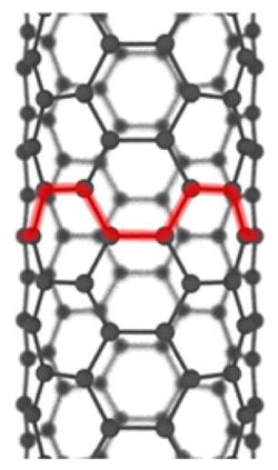
Research on carbon materials in the Condensed Matter group focusses on carbon nanotubes and graphene. Carbon exists in many allotropic forms, but these two materials provide naturally-occurring examples of low-dimensionality combined with high crystalline purity, allowing access to several exotic quantum phenomena.
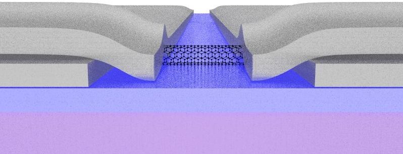
As components in the types of device used in spintronics research carbon nanotubes and graphene both offer long spin coherence times, meaning that information encoded using the spin on an electron can be retrieved from a device following processing. The lack of scattering in carbon nanotubes also makes them viable components in more advanced quantum information devices, where electrons are entangled. In the Condensed Matter Group we fabricate nanoscale devices in order to access these quantum phenomena - a device schematic is shown below.


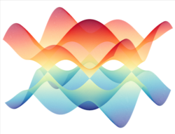
Graphene offers similar benefits in terms of spin coherence, combined with relative ease of processing due to its 2D nature. As a result of its unique band-structure (right), electrons in graphene also have the unusual property of being 'massless' and their behaviour is best described using relativistic equations, giving experimental access to a variety of novel physics.
In order to manufacture large or complex devices, or for technological applications, it is necessary to grow large areas of graphene, not possible using the pioneering technique used for the work leading to the Nobel Prize for physics in 2010. We grow graphene from a silicon carbide substrate, using an anneal at high temperatures and under ultra-high vacuum conditions to cause Si atoms to sublime from the surface layers of the crystal, leaving an excess of carbon atoms which then form a layer of graphene.
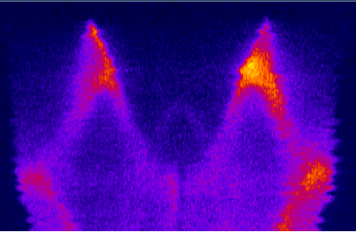
The substrates used measure 5mm by 10mm, but the graphene formed (to date) is not a single crystal, but consists of many domains. We use surface science techniques such as LEED, Raman microscopy, AFM and STM as well as low-temperature electronic measurements to link the surface morphology to the electronic properties. We also visit the National Synchrotron Light Source at Brookhaven in the USA to image the graphene surface using LEEM, and to map the band structure using ARPES, shown below.


