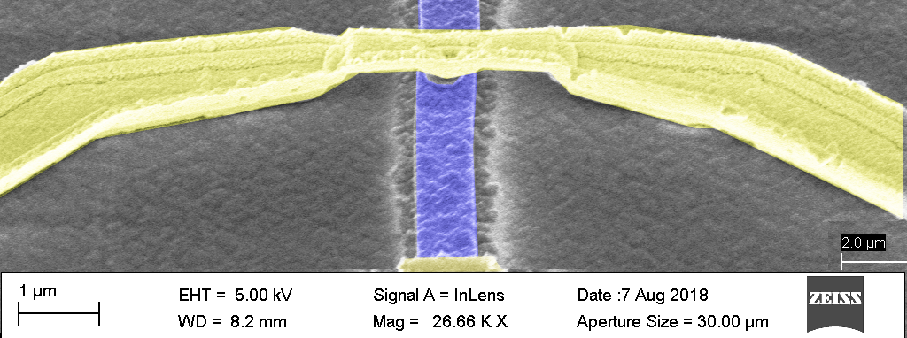
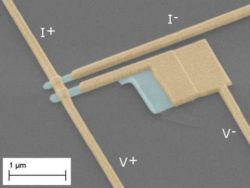
Fabrication Facilities
The group makes use of the University's Wolfson cleanrooms that are housed on campus in the Electrical Engineering department. The cleanroom has facilities for photolithography, electron-beam lithography and focused-ion-beam lithography as well as standard wet and dry etching processes. In addition, the group posseses a Nanoprobe system containing an SEM column and four scanning probe tips.
Photolithography
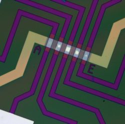 Photolithography is a process akin to printing and developing photographs. A pattern is created using a mask to expose regions of a photosensitive polymer to a UV light source. The polymer is then developed in a chemical solution that removes all exposed regions, leaving behind a template pattern identical to the original mask. Thin films are deposited through this template to form device structures. The University of Leeds cleanrooms are equipped with three Karl Suss MJB3 Contact mask aligners for performing photolithography with feature sizes down to ~800nm.
Electron-beam lithography
A process similar to photolithography, except that a focussed beam of electrons is used to expose the resist, rather than photons. Complex geometrical patterns can be created by steering the beam across the surface of the sample. The electron beam lithography system in our cleanrooms is a Raith 50 system which is based on a SEM system with additional hardware and pattern generating software. The system can produce structures with a minimum feature size of around 50 nm.
Focussed Ion beam lithography
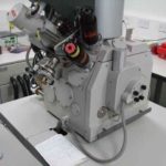 In a focussed ion beam system a beam of Ga+ atoms is incident on the surface of the sample. The impact of the high energy Ga+ ions causes atoms to be ejected from the surface. By steering the ion beam around the surface of the sample, it is possible to direct the milling process to selectively remove material from the sample. The cleanroom houses a FEI Novalab 200 Dual SEM-FIB system. This state of the art system comprises a very high quality FEG-SEM column and a Ga focused ion beam column that can image the same sample simultaneously.
The Omicron Nanoprobe
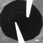 This system is unique in the UK as being a combination of a high-resolution SEM column and 4 STM probes in one system. The Nanoprobe can be used to manually assemble devices – for example to directly place carbon nanotubes onto patterned contact pads.
For a tutorial on patterning thin films, please click here.

